„Hex Buffer” változatai közötti eltérés
Nincs szerkesztési összefoglaló |
|||
| 19. sor: | 19. sor: | ||
Logic Case Style: DIP | Logic Case Style: DIP | ||
No. of Pins: 16 | No. of Pins: 16 | ||
[[Fájl:74hc4050.jpg|bélyegkép|balra|74hc4050.jpg]] | |||
[[Fájl:74hc4050.jpg|bélyegkép|74hc4050.jpg]] | |||
A lap 2017. szeptember 24., 11:34-kori változata
Hex Buffer
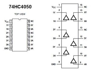
74HC4050 Hex Non-Inverting Buffer
The 74HC4050 chip has an input protection structure that makes these chips ideal as logic level translators which convert high-level logic to a low-level logic while operating off the low-level logic supply.
For example, 5V input pulse levels can be down-converted to 3.3V logic levels. These parts also can be used as simple buffers without level translation.
The buffer on these chips is one way. I.e. the input voltage controls the output voltage. You cannot control the input from the output. This makes these chips ideal for logic level conversion when using the SPI bus, but they wont work for I2C as this requires bi-directional logic level conversion.
The 74HC4050 is fabricated with high-speed silicon gate technology
Supply Voltage Range: 2V to 7V Input Voltage Range: -0.5V to 16V Logic Case Style: DIP No. of Pins: 16
